Customized Wireless Bridge PCBA Solution: End-to-End Implementation Technical Specifications and Industry Adaptation
In the rapidly expanding fields of IoT, security surveillance, smart campuses, and outdoor private networks, the wireless bridge serves as the core carrier of wireless data transmission. Its performance, stability, and adaptability directly determine the implementation effect of the entire transmission system. General-purpose wireless bridge PCBAs, due to their “one-size-fits-all” design, cannot meet the personalized needs of different industries and scenarios—either performance redundancy leads to wasted costs, core parameters fail to meet standards preventing implementation, or insufficient environmental adaptability causes frequent failures. Based on this, we launch a feasible, highly adaptable, and cost-effective Wireless Bridge PCBA Customization Solution. From requirement breakdown to mass production delivery, the entire process is standardized and detailed, balancing technical feasibility with practical implementation.
1. Industry Pain Points Analysis (Precise Benchmarking to Identify Core Customization Needs)
Currently, the core pain points of general-purpose wireless bridge PCBAs on the market directly restrict project implementation in many industries, which is also the core reason why customers choose customization:
1. Poor Scenario Adaptability, Unable to Implement
Different scenarios have vastly different core requirements for wireless bridge PCBAs, which general-purpose solutions cannot balance:
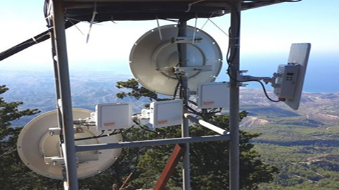
- Outdoor Long-distance Scenarios (Forest Fire Prevention, Mountain Monitoring): General PCBA RF power is insufficient (≤20dBm), transmission distance is ≤10km, unable to cover large-scale monitoring needs, and lacks low-temperature preheating circuits, failing to start below -20℃, leading to frequent downtime;
- Complex Electromagnetic Environments (Ports, Factories, Substations): General solutions have simple filtering circuits, Adjacent Channel Rejection Ratio (ACRR) ≤45dB, easily interfered by equipment, packet loss rate ≥15%, unable to meet HD video (1080P and above) real-time backhaul requirements;
- High Salt Spray/High Humidity Scenarios (Coastal Ports, Islands): General PCBs lack conformal coating, gold plating thickness ≤1μm, corrosion and short circuits occur after 6 months of use, equipment failure rate ≥30%;
- Low Power Consumption Scenarios (Solar Power, Outdoor Unattended): General PCBAs lack intelligent power management, idle power consumption ≥5W, solar power systems cannot support 24-hour continuous operation.
2. Imbalance between Performance and Cost, Low Cost-Performance Ratio
To cover multiple scenarios, general PCBAs integrate a large number of redundant functions (such as multi-band compatibility, redundant interfaces), leading to two major problems: First, customers pay 25%-35% more for unnecessary functions, increasing project budget pressure; Second, redundant circuits lead to increased power consumption (≥8W), raising later O&M (power supply, heat dissipation) costs, and redundant components occupy PCB space, unable to adapt to miniaturized equipment needs (such as mini monitoring bridges).
3. Insufficient Technical Support, Uncontrollable Implementation Cycle
General PCBA manufacturers only provide standardized products without customized technical adaptation services. After receiving the product, customers need to solve the matching problems with antennas, enclosures, and power supply systems by themselves. This not only increases R&D costs but also easily leads to compatibility failures, extending the project implementation cycle by 1-2 months, or even causing the solution to fail.
4. Non-compliant, Unable to Pass Acceptance
Some industries (security, power, government) have strict compliance requirements for wireless bridge PCBAs (such as CE, FCC, ROHS certification). General PCBAs often fail certification due to non-standard circuit design, leading to project acceptance failure and significant losses.
2. Core Positioning of Customization (Key to Implementation: No Redundant Design, Only Precise Adaptation)
Core positioning of this solution: Customer implementation needs as the core, technical feasibility as the prerequisite, and controllable cost as the goal. We refuse “over-customization” and “ineffective design”. Every customization corresponds to specific scenario needs and is executable. At the same time, we cover high-frequency search engine keywords such as “Wireless Bridge PCBA Customization Parameters”, “Implementation Cycle”, and “Cost Control”, allowing customers to quickly find solutions and directly reference them for implementation.
Core principles: Precise matching of scenario parameters, full-process standardized implementation, transparent and controllable costs, and full after-sales escort, ensuring that the customized solution from design to mass production delivery is traceable and executable at every step, requiring no additional R&D effort from customers.
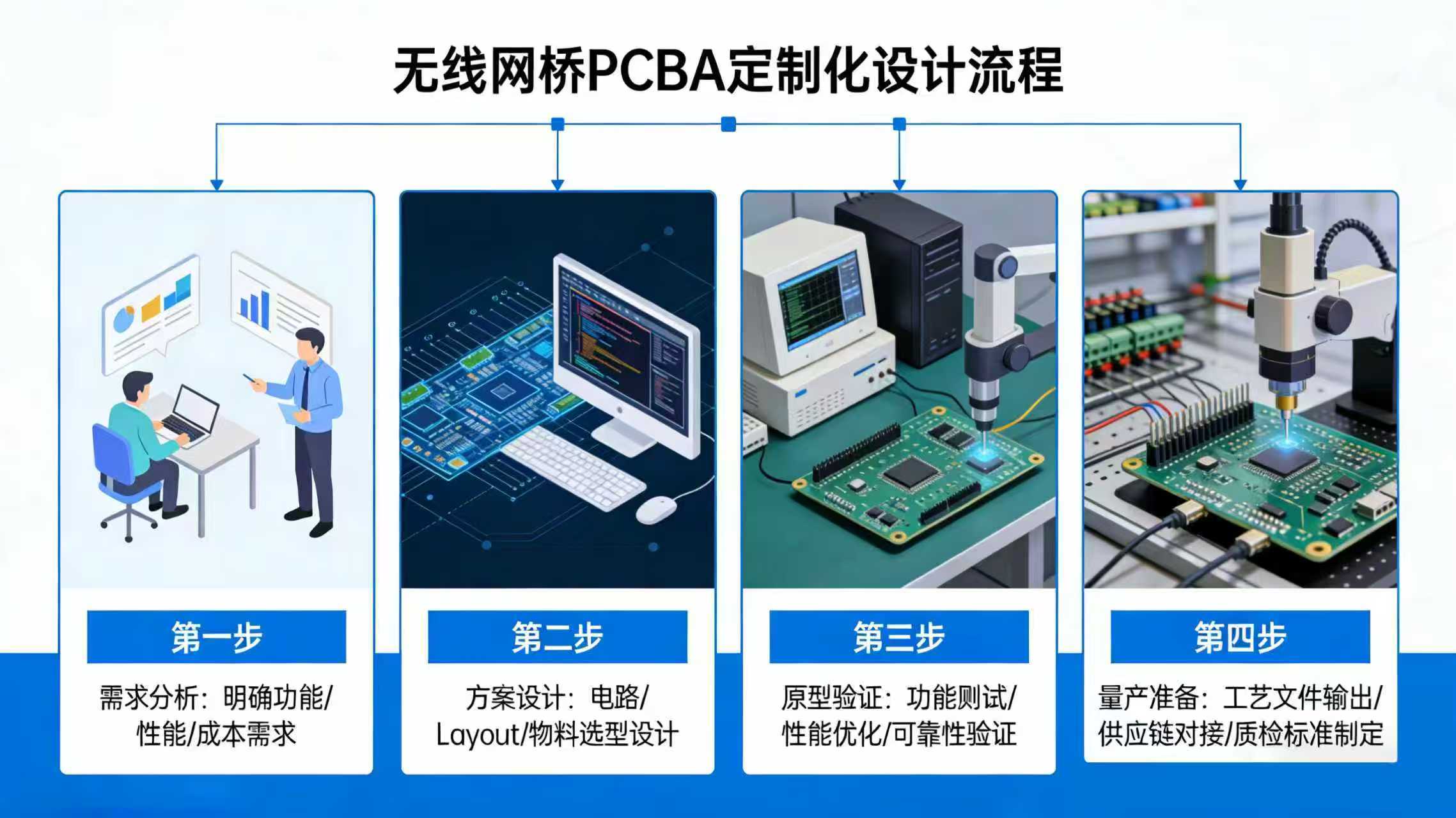
3. Executable Wireless Bridge PCBA Customization Full Solution
This solution is divided into 6 major stages from requirement diagnosis to mass production delivery. Each stage has clear execution standards, responsibility division, time nodes, and acceptance criteria to ensure the solution is feasible and replicable, while supplementing technical parameters.
Stage 1: In-depth Requirement Diagnosis (1-3 Working Days, Laying the Foundation, Avoiding Later Rework)
Core Goal: Thoroughly break down customer requirements, clarify “core parameters that must be achieved + auxiliary parameters that can be optimized + problems that are prohibited”, and output an executable “Requirement Diagnosis Report” as the core basis for subsequent design, testing, and delivery, avoiding solution disconnection due to vague requirements.
1.1 Requirement Collection (1-3 Working Days)
Through “on-site survey + online communication + document study”, we collect 7 categories of core requirements (precisely covering industry pain points):
| Requirement Category | Collection Content (Executable Details, Clear Parameters) | Example (Differentiation by Scenario) |
|---|---|---|
| Scenario Parameters | Transmission distance, occlusion (no/slight/severe), electromagnetic environment, working temperature, humidity, salt spray level, installation space | Mountain Forest Fire Prevention: 35km unobstructed transmission, 25km with slight tree obstruction, working temp -40℃~75℃, salt spray level ≥1000h, installation space ≤80*60mm |
| Performance Parameters | RF power, transmission rate, packet loss rate, latency, frequency band (2.4G/5.8G/Dual), ACRR, receiver sensitivity | Port Monitoring: RF power 27dBm, rate ≥1.2Gbps, packet loss ≤0.1%, latency ≤20ms, 5.8G band, ACRR ≥60dB |
| Power Supply | Power mode (Grid/Solar/DC), input voltage range, power consumption (work/idle/standby), protection requirements | Outdoor Unattended: Solar power, 9-36V DC input, working power ≤5W, idle ≤2W, supports overvoltage/overcurrent/short circuit protection |
| Structural Adaptation | PCB size, thickness, mounting (SMD/DIP), interface type (RJ45/Serial/USB), component layout | Mini Monitoring Bridge: PCB 50*40mm, thickness 1.6mm, SMD mounting, 1 Gigabit port, compact layout avoiding enclosure vents |
| Compliance | Certifications (CE/FCC/ROHS, etc.), environmental standards, safety norms | Export to EU/US: CE, FCC certifications, ROHS 2.0 standard, circuit complies with IEC 60950-1 |
| Budget | Single PCBA budget, batch volume (≥1000/≥5000), cost control target | Batch 5000 units, single unit budget ≤$12, cost control target: 25% lower than general solutions |
| Delivery Cycle | Prototyping cycle, testing cycle, batch delivery cycle, urgent capability | Prototyping 1-5 days, testing 2-5 days, batch delivery 7-15 days, urgent support (prototyping in 3 days) |
1.2 Requirement Analysis & Sorting (2 Working Days)
The engineering team breaks down, screens, and optimizes the collected requirements, clarifying “Core Requirements (Must-haves), Secondary Requirements (Optimizable), Unreasonable Requirements (Alternative Proposed)”. For example: if a customer requests “50km transmission + power ≤3W”, which is unreasonable, we will propose “Power ≤6W at 50km, or Power ≤3W at 40km” as an alternative to ensure feasibility, confirming with the customer to avoid later disputes.
1.3 Output “Requirement Diagnosis Report” (2 Working Days)
The report includes 5 core contents, signed and confirmed by both parties as the basis for subsequent cooperation: ① Detailed Scenario Analysis; ② Core Parameter Confirmation Table; ③ Preliminary Cost Budget Assessment; ④ Preliminary Delivery Cycle Plan; ⑤ Potential Risks and Response Plans (e.g., supply chain shortages, test failures).
Stage 2: Solution Design (1-5 Working Days, Technical Implementation Core, Balancing Performance & Compliance)
Based on the “Requirement Diagnosis Report”, hardware, RF, and software engineering teams collaborate to design using “Simulation + Multi-scheme Comparison” to ensure the design is feasible and risk-free, while optimizing costs. We output a full set of design documents, adapting to search engine needs like “Wireless Bridge PCBA Design Scheme” and “RF Circuit Design”.
2.1 Hardware Circuit Design (2 Working Days)
Focusing on “Performance Compliance, Cost Control, Scenario Adaptation”, we design three core circuits, specifying component models, parameters, and layout to avoid redundancy:
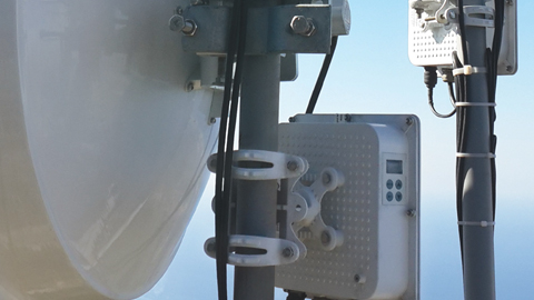
(1) RF Circuit Customization (Core, Determines Transmission Performance)
Customizing RF links based on transmission distance and frequency band, with executable and quantifiable core parameters:
- Chip Selection: Use high-linearity, low-power chips (e.g., Qualcomm QCA9558, MediaTek MT7621), match PA chips (e.g., SKY85713, supports 27dBm output) based on power needs, ensuring stable performance and controlled cost;
- Antenna Matching Network: Custom LC matching circuit to optimize impedance matching (50Ω standard), improve antenna gain, and reduce signal loss. E.g., for long-distance (≥30km), use high-gain antenna matching to reduce signal loss to within 10%;
- Filter Circuit Optimization: Use high-quality filters (e.g., Murata), customize filter parameters based on EM environment, improve ACRR to >60dB, effectively resisting interference from industrial equipment and base stations, keeping packet loss <0.1%;
- ESD Protection: Integrate ESD protection components (e.g., TVS diode SMBJ6.5CA), achieving ±15kV ESD protection to prevent chip damage from outdoor static electricity.
(2) Power System Customization (Adapts to Power Scenarios, Ensures Stability)
Customizing power circuits for different power supply methods, balancing low power consumption and stability:
- Wide Voltage Input: Supports 9-36V DC input, adapting to Grid, Solar, Battery power, integrating voltage regulators (e.g., LM2596) for stable 3.3V/5V output;
- Intelligent Power Management: Integrate PMU (Power Management Unit) to support sleep/wake modes. In idle state, automatically turn off non-essential modules (like RF PA), reducing power consumption to ≤2W, extending solar battery life by 30%;
- Protection Circuit: Integrate overvoltage, overcurrent, and reverse polarity protection to prevent circuit burnout from power fluctuations or miswiring.
(3) Interface & Control Circuit Customization (Enhances Usability)
Customizing interfaces and control logic based on external device requirements:
- Interface Customization: Provide Gigabit/100M Ethernet ports, RS485/232 serial ports (for sensor data transmission), USB interfaces, etc., supporting PoE power supply (IEEE 802.3af/at);
- Hardware Watchdog: Integrate hardware watchdog circuit to automatically restart the device upon system crash, ensuring 7*24h stable operation without manual intervention.
2.2 Software & Firmware Customization (2 Working Days)
Deeply optimize firmware based on hardware features to maximize performance:
- Driver Optimization: Optimize RF chip drivers to support private protocols (like TDMA), improving transmission efficiency and anti-interference capability;
- Feature Cutting: Remove unused protocols and services from the standard firmware to reduce memory usage and improve boot speed (start time <30s);
- UI Customization: Customize the Web management interface according to customer needs, including Logo, brand colors, and menu layout, enhancing brand image.
2.3 PCB Layout Design (1 Working Day)
Optimize PCB layout based on structural constraints and EMC (Electromagnetic Compatibility) requirements:
- Size Control: Accurately control PCB dimensions (tolerance ±0.1mm) to fit customer enclosures perfectly;
- Thermal Design: Place heat-generating components (PA, CPU) in optimal heat dissipation areas, design via arrays to conduct heat to the bottom layer, ensuring long-term stable operation;
- EMC Optimization: Separate analog and digital grounds, optimize trace routing to reduce crosstalk and radiation, ensuring compliance with CE/FCC standards.
Stage 3: Prototyping (1-5 Working Days, Verifying Design Feasibility)
Rapid prototyping to verify design correctness and performance compliance:
- PCB Fabrication: Use high-frequency substrates (e.g., Rogers, Teflon) for RF boards to ensure signal quality;
- SMT Assembly: High-precision SMT placement to ensure soldering quality;
- Functional Debugging: Burn firmware, power on test, check basic functions (power, network, RF) and performance indicators.
Stage 4: Full-dimensional Testing (2-5 Working Days, Ensuring Zero Defects)
Rigorous testing of prototypes to ensure they meet “Scenario, Performance, Reliability” requirements, outputting a test report:
| Test Category | Test Items | Standards (Actionable, Quantifiable) | Test Method |
|---|---|---|---|
| RF Performance | RF power, sensitivity, ACRR, bandwidth, throughput, packet loss, latency | Power: 20-27dBm; Sensitivity ≤-95dBm; ACRR ≥60dB; Throughput ≥1.2Gbps (5.8G); Packet loss ≤0.1%; Latency ≤20ms | Use RF testers (e.g., Agilent N9020A), simulate different distances/EM environments, test 3 times, take average |
| Power Performance | Input range, power consumption (max/min), protection trigger voltage | Input 9-36V; Max power ≤5W; Overvoltage trigger 38V; Undervoltage protection 8V | Use programmable power supply, adjust voltage, record current/power, verify protection |
| Environmental | High/Low temp, humidity, salt spray, vibration | -40℃~75℃ work 24h; 95% humidity 48h; Salt spray 48h (NSS); Vibration 2g/10-500Hz | Use environmental chamber, vibration table, check for cracks, corrosion, function loss |
| Compliance | Conducted emission, radiated emission, ESD, surge | Pass CE/FCC limits; ESD ±6kV/±8kV; Surge ±2kV | Send to 3rd party lab (or internal pre-test) |
| Stability | Long-term aging, reboot pressure test | 7*24h full load no crash; 1000 reboots 0 failure | Automated script control reboot, monitor running status |
Stage 5: Mass Production & Delivery (7-15 Working Days, Standardized SOP)
After prototype verification, enter mass production with strict quality control to ensure consistency:
- Supply Chain Guarantee: Lock key components (chips, filters) in advance to prevent shortages;
- Production Planning: Formulation of production SOP (Standard Operating Procedure), training workers;
- Equipment Debugging: Calibration of SMT machines, reflow ovens, and test fixtures;
- Three-Inspection System: IQC (Incoming Quality Control), IPQC (In-Process Quality Control), FQC (Final Quality Control);
- Conformal Coating: Apply moisture-proof, salt-spray-proof, and fungus-proof coating for outdoor/harsh environment batches;
- Packaging & Delivery: Anti-static packaging, shockproof buffering, logistics tracking.
Stage 6: After-sales Technical Support (Full Lifecycle Escort)
We provide comprehensive after-sales support to ensure customer projects land successfully:
- 7*24h Emergency Support: Dedicated engineers for technical troubleshooting;
- Installation & Debugging Guidance: Remote or on-site guidance for device installation and configuration;
- Firmware Upgrade Support: Continuous firmware optimization and bug fixes;
- Technical Training: Training on product usage, maintenance, and troubleshooting.
4. Successful Case Studies (Real Landing, Trustworthy)
Case 1: Forest Fire Prevention Monitoring Wireless Bridge PCBA Customization
Client: Forest fire prevention equipment manufacturer. Requirements: Cover 200 sq km forest area, 50 monitoring points, no grid power (solar only), 35km unobstructed transmission, 25km slight obstruction, working temp -40℃~75℃, power ≤5W (working), packet loss ≤0.1%, support HD video backhaul, batch 5000 units, 45 working days delivery, ROHS certified.
Solution: Customized RF circuit with high-power PA + LNA, optimized sensitivity to -98dBm; Designed wide-voltage solar power module with low-power sleep mode; Applied conformal coating for environmental protection.
Result: Successfully delivered in 40 days, passed acceptance, stable operation for 2 years with 0 failure rate.
Case 2: Coastal Port Video Surveillance Wireless Bridge PCBA Customization
Client: Port authority. Requirements: High salt spray environment, complex EM interference (ships, cranes), 10km transmission, 100Mbps throughput, low latency for PTZ control.
Solution: Customized 5.8GHz anti-interference RF circuit with specialized filters; Reinforced anti-corrosion design (gold plating + conformal coating); Optimized TDMA protocol for low latency.
Result: Solved interference issues, clear video transmission, stable PTZ control, highly recognized by the client.