PCBA Frequently Asked Questions Manual and Troubleshooting
News 2026-02-14
PCBA FAQ & Troubleshooting Handbook
Foreword: This handbook answers the most common questions about PCBA (Printed Circuit Board Assembly) during technical consultation, installation, commissioning, and after-sales maintenance. It provides a quick reference for engineers, installers, and managers to improve efficiency and reduce failures and losses caused by improper operation or misunderstanding. Content is organized into Technical, Installation, and After-Sales categories for clarity and accuracy.
1. Technical FAQs
1.1 What is PCBA? How is it different from PCB?
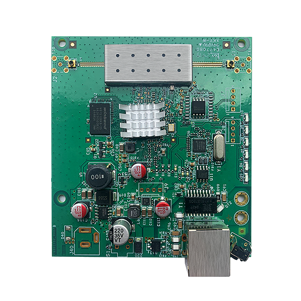
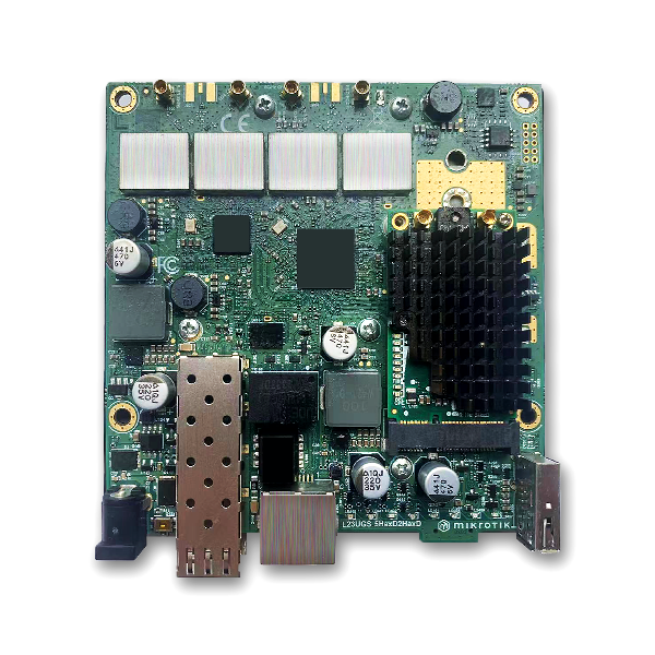
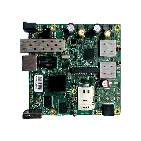
Answer: PCB (Printed Circuit Board) is a bare board with copper traces and pads, without electronic components. PCBA (Printed Circuit Board Assembly) is a finished board with all components mounted and soldered, ready for use in electronic devices. Simply put: PCB = bare board; PCBA = assembled and functional board.
1.2 What are common PCBA base materials and their applications?
Answer: Common materials include FR-4, FR-1, CEM-1, and metal-core substrates. Key differences:
- FR-4: Epoxy glass laminate, high Tg (≥130°C), strong insulation and mechanical strength. Most widely used for consumer electronics, industrial control, communications;
- FR-1: Phenolic paper laminate, low cost, lower heat resistance (Tg ≤100°C). Used in low-cost devices such as toys and chargers;
- CEM-1: Composite epoxy material, performance between FR-1 and FR-4. Balances cost and performance;
- Aluminum PCB: Excellent thermal conductivity. Used for high-power, high-heat applications such as LED drivers and power boards.
1.3 What are the main PCBA soldering processes?
Answer: Primary processes are Reflow Soldering, Wave Soldering, and Manual Soldering:
- Reflow Soldering: For SMD components. Solder paste is printed, components placed, then heated in a reflow oven. High efficiency, consistent joints; high equipment cost, not for through-hole;
- Wave Soldering: For through-hole and mixed technology. Board passes over molten solder wave. Good for through-hole; lower consistency, risk of bridging;
- Manual Soldering: For prototypes, small batches, rework. Flexible, no large equipment; low efficiency, quality depends on operator skill.
1.4 What causes cold joints / false soldering? How to prevent them?
Answer: Main causes and prevention:
- Cause 1: Poor solder paste (expired, oxidized, uneven printing). Use qualified paste, follow shelf life, control printing parameters;
- Cause 2: Oxidation or contamination on leads or pads. Clean components, use anti-oxidation finishes (HASL, ENIG), wear ESD gloves;
- Cause 3: Incorrect temperature or time. Set proper reflow/wave profile; manual soldering: 260±20°C, ≤3 seconds per joint;
- Cause 4: Misalignment. Ensure component pins align accurately with pads.
1.5 What are ESD requirements for PCBA?
Answer: Static electricity damages ICs, MOSFETs, and sensitive components. Strict ESD protection is required:
- Environment: ESD floor, mat, ion fan; humidity 40%–60%;
- Personnel: ESD wrist strap (grounded), gloves, garments; no bare-hand contact;
- Storage: Use anti-static bags and bins;
- Grounding: All equipment grounded; resistance ≤4Ω.
1.6 What tests are performed on PCBA?
Answer: Tests ensure quality and function:
- General: Visual inspection, continuity/open/short test, solder joint strength;
- Special: Insulation resistance, Hi-Pot, functional test, temperature/humidity aging.
1.7 How to check if a component is damaged?
Answer: Visual inspection + instrument test:
- Visual: Swelling (capacitors), burning, cracking, broken leads, lifted pads;
- Instrument: Multimeter for resistance, capacitance, diode values; oscilloscope for signals; functional test fixture for complex issues.
2. Installation FAQs
2.1 Preparation before PCBA installation
Answer: Proper preparation prevents damage:
- Environment: Clean, dust-free, ESD-safe;
- Material: Verify model, version, accessories;
- Tools: Proper ESD screwdrivers, tweezers;
- Personnel: ESD protection, familiar with procedure.
2.2 Screw mounting precautions
Answer: Improper mounting causes bending, pad lift, or short circuit:
- Screw size: Match hole and length; avoid too long/short;
- Torque: Tighten evenly; 0.5–1.5N·m recommended;
- Insulation: Use washers near circuits if needed;
- Sequence: Tighten diagonally to avoid warping.
2.3 How to avoid component damage during installation?
Answer:
- Avoid pressing or touching components directly;
- Use proper tools; do not pull wires or pins;
- Install in correct orientation;
- Maintain full ESD protection.
2.4 Connecting PCBA to housing, cables, etc.
Answer:
- Cables: Match connectors, insert fully; pull by housing, not wire;
- Housing: Avoid sharp edges; allow heat dissipation;
- Environment: Use seals/gaskets for dust and moisture protection.
2.5 Multi-PCBA assembly guidelines
Answer:
- Use positioning holes and pins for alignment;
- Ensure connectors and cables are secure;
- Distribute stress evenly to avoid bending.
2.6 Checks before powering on
Answer:
- Visual: No damage, loose parts, proper connections;
- Continuity: Check for short/open circuits;
- Voltage: Match rated power;
- Ground: Good chassis ground, resistance ≤4Ω.
3. After-Sales & Troubleshooting
3.1 PCBA has no response when powered on
Answer: Troubleshoot in order (disconnect power first):
- Check input power, adapter, cables, and connectors;
- Check power input, switch, fuse, and power paths;
- Inspect power ICs, capacitors, MOSFETs for damage;
- Verify ground connection.
3.2 Unstable operation: freezing, rebooting
Answer:
- Check power stability;
- Check heat dissipation; clean or upgrade heatsinks;
- Check loose connectors and mounting;
- Check aged components (especially capacitors).
3.3 How to locate a short circuit quickly?
Answer: Disconnect power immediately.
- Visual inspection for burning or charring;
- Multimeter in beep mode; isolate components one by one;
- Use test fixture for batch issues;
- DO NOT power on until short is fixed.
3.4 Component or pad fallen off? How to repair?
Answer:
- Component fallen: Clean pad, re-sell or replace component;
- Pad lifted: Repair by wire-jump to inner trace; replace board if badly damaged.
3.5 Performance degradation over time
Answer:
- Component aging (caps, resistors); replace worn parts;
- Moisture, dust, corrosion; clean with alcohol, improve sealing;
- Dust buildup; clean regularly to restore cooling.
3.6 Warranty terms
Answer:
- Warranty: 1–2 years consumer; 2–3 years industrial (per contract);
- Covered: Manufacturing defects, component quality issues;
- Not covered: Misuse, improper installation, ESD damage, unauthorized modification, environmental damage.
3.7 What information is needed for RMA?
Answer:
- Required info: PCBA model, version, batch; equipment model; failure details; operating conditions;
- Process: Contact support → initial diagnosis → return → repair → test → return to customer.
3.8 How to extend PCBA service life?
Answer:
- Environment: Dry, clean, ventilated; -20°C to 60°C, humidity 40–60%;
- Operation: Follow procedures; avoid stress/vibration;
- Maintenance: Regular cleaning, inspection, replacement of worn parts;
- ESD: Always protect against static damage.
4. Supplementary Terms
1. This handbook covers common issues only. For special or complex failures, contact technical support for professional assistance.
2. Content will be updated periodically as technology and applications evolve.
3. If conflicts exist between this handbook and the product manual or contract, the official manual and contract shall prevail.